
STM Tip Preparation
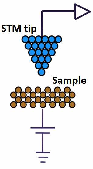
For maximum resolution in a scanning tunneling microscope (STM), an extremely sharp metallic tip is required, which serves as the point through which the STM “scans” a sample. A blunt tip reduces STM resolution, because it can cause electron tunneling to occur across a wider spatial range than intended. One of the most commonly used methods to create such a tip is electrochemical etching of a metal wire.
The process of electrochemical etching involves applying a potential difference between a cathode and the metal wire through a basic solution. The wire is etched away at the meniscus of the solution, until the weight of the submerged wire is greater than the tensile force at the etching point. The wire then breaks at the meniscus and an STM tip is created. If the voltage continuous to be applied after this, the tip would get etched further, and become more blunt. To prevent this from happening, a cut-off circuit was created to detect the breaking of the wire and to stop the etching process. In order to create a sufficiently sharp tip, the etching process must be cut off as soon as possible once the tip is formed. A typical benchmark for a good STM tip is a radius of curvature of 50 nm or less at the tip apex. The sharpness of the tip is dependent on the operation of the cut-off circuit and is limited by the speed of the circuit itself.
Etching Process
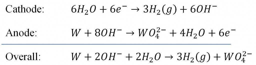
Equations above describe the etching process of a tungsten (W) wire in a basic solution (Ibe et al., Journal of Vacuum Science Technology, A 8, 3570 (1990)). Using this method, the wire is etched near the meniscus until the weight of the wire is large enough to cause the wire to break at the etching point. The majority of etching will happen at exactly at this point, with very little etching happening below. During the etching process, bubbles are expected to form around the cathode, but should not form around the tip itself. If they do form around the tip wire itself, then the voltage must be reversed (wires connecting the cathode and the W wire should be switched). The voltage at the cathode will most likely read around 9-10 V, while the voltage at the tip will be closer to 11 V. A complete etching cycle typically takes 15-20 minutes.
It is important to note that a tungsten oxide layer is formed during this process. This oxide layer is presumably the reason why etching is mostly isolated at the meniscus of the solution – as the tungsten gets etched, this oxide sinks and forms a protective coating around the rest of the submerged wire (Ibe et al., Journal of Vacuum Science Technology, A 8, 3570 (1990)). Although the oxide does not block 100% of the etching, it does block a significant amount, and it is possible to see the oxide coating the tip and sinking in the water during the etching process.
Circuit Design

The circuit used to cut off the etching process is shown on the left. It uses a comparator to compare a user set reference voltage with the voltage across the metallic cathode in the solution. This circuit was designed with a 0.25 mm diameter W wire in mind, with a stainless steel foil tube cathode surrounding the tip, and a basic solution of NaOH. As the tip is etched, the resistance of the tip in the solution (the load) goes up. This increase in load drops the voltage across V_in- of the comparator. Once the tip breaks, the resistance suddenly increases, and the reference voltage becomes higher than the voltage across the load. At this moment, the comparator shuts off the circuit by switching a MOSFET transistor, effectively removing any voltage across the load. The key to creating a sharp tip is to have the reference voltage as close as possible to the voltage across the load at the moment the tip drops. For example, if, at the moment the tip drops, the voltage across the load is 450 mV, then a reference voltage of 445 mV would create a sharp tip, but a reference of 200 mV would leave a large gap in between the tip breaking and the circuit shutting off, creating a blunt tip.
Circuit operation is controlled with a 3 way kick starter switch. Position 1 of the switch is a 5v kick start, while position 3 grounds the circuit, thus turning it off. In order to start the circuit, simply turn on the 5v for a few seconds and then move the switch into the neutral position for the remaining duration of the etching process. When the circuit is off, an LED will turn on and a buzzer will sound (can be disabled). The reference current is set with a 10 turn precision potentiometer, and the voltage across the load can be adjusted by a single turn input gain potentiometer.
Recommended etching conditions
We use 0.25 mm diameter tungsten (W) wire, a stainless steel cylinder-shaped cathode, and a 2M NaOH solution. The factors that affect tip sharpness include: input gain, reference voltage, and tip depth. Sharp tips have been made in our lab with an input gain of 950 mV and a reference voltage of 450 mV, with a tip depth of approximately 2-3 mm. The input gain will affect the exact reference voltage required – for a higher input, a higher reference voltage will be required to create an equivalent tip. If the reference voltage is set too high, the circuit will cut off before the etching process is complete and the tip “drops”. This is not an entirely bad situation, as a simple restart of the circuit along with a readjustment of the reference voltage is enough to set the circuit back on track. However, if, during this restart, the tip drops during the time in which the +5v kick starter is activated, the comparator will not switch off the circuit until the +5v is turned off – thereby defeating the purpose of the circuit and blunting the tip. In this case, the tip is almost guaranteed to be blunt, and should be discarded. If the reference voltage is set too low, the time it takes to shut off the circuit after drop will be increased, etching a blunter tip.
Tip depth should be set so that the end of the tip wire is 2-3 mm below the meniscus.
1) If the wire is not sufficiently submerged, the weight of the tip below the etching point at the meniscus will never be greater than the tensile force, preventing the tip from breaking. As mentioned above, the majority of the etching occurs at the meniscus. However, due to the slight amount of etching that does occur, if the tip is not submerged deep enough into the solution, the entire submerged piece of wire will be etched before the wire breaks – thus creating no tip at all.
2) If the wire is submerged too far into the solution, a “rebound” effect is created, where during the break, the etched tip snaps back like a rubber band due to the excess amount of weight below the breaking point. This creates a curved tip or a tip with a deformity at the end. This deformity is only large enough to be seen under a scanning electron microscope (SEM), but will render the tip worthless.
3) For a similar reason, to minimize the rebound effect at all tip depths and to create an evenly etched tip, tip wire needs to be inserted into the solution perpendicularly to the sample surface.
Tip storage, cleaning, and SEM imaging
As STM tips can be damaged easily, they should be stored in a closed container. Light weight foam can be used to insert the back end of a tip and store it. Over time, an oxide layer forms over the tips, due to their contact with air. This oxide layer will lower the tip quality. To prevent the oxide layer from forming, it is possible to store the tips on top of soft polyurethane and submerge the polyurethane into acetone or isopropanol. This will prevent any contact with oxygen. Using either of these two solutions will require a sealed, air tight container, as both substances evaporate very quickly.
Regardless of the storage method, STM tips must be cleaned before use. One way to do this is to submerge the tips in hydrofluoric acid, which removes any contamination or oxide layer on the tip. Subsequently, the tips are also annealed at high-temperature in ultra-high vacuum to remove any remnant oxide layer, before they are inserted into the STM head and used for measurements. Radius of tip curvature achieved with the setup described above was less than 50 nm.
The content on this page is a modified version of a lab report written by Ishaan Bhojwani, a high school student and a summer intern in Zeljkovic Lab in 2015.