
Scanning Tunneling Microscopy (STM)
Basic Principles
Scanning tunneling microscopy (STM) is an experimental technique based on the principles of quantum tunneling of electrons between two electrodes separated by a potential barrier, typically used for imaging surfaces of materials with sub-atomic resolution. It was pioneered by Gerd Binnig and Heinrich Rohrer in 1982, and was awarded a Nobel Prize in Physics in 1986.Typical STM experimental setup consists of a sharp metallic tip which is brought within several angstroms of a conducting surface using a 3-dimensional piezoelectric scanner (Figure 1(a)). This scanner can position the tip both laterally (in the xy – plane) and vertically (in the z – direction) with sub-angstrom precision. Application of voltage V between the tip and the sample allows electrons to quantum-mechanically tunnel between the two (Figure 1(b)). The resulting tunneling current can be calculated using the time-dependent perturbation theory. If a positive V is applied to the sample, the Fermi level of the sample shifts down with respect to the Fermi level of the tip, and electrons tunnel from the occupied states of the tip into the empty states of the sample (Figure 1(b)).
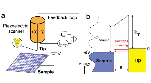
Figure 1. Basic principles of STM and STS. (a) Schematic representation of STM. A voltage V is applied between the tip and the sample. The tip is rastered across the surface in the xy plane and its z coordinate is adjusted using the three-dimensional piezoelectric scanner controlled by a feedback loop. (b) Quantum tunneling of electrons between the tip and the sample across a vacuum barrier of width s upon the application of a voltage bias V between the two. If a positive V is applied to the sample, the Fermi level of the sample shifts down with respect to the Fermi level of the tip, and electrons tunnel from the occupied states of the tip into the empty states of the sample.
STM Tunneling Equation
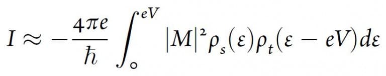
The contribution to the tunneling current from tunneling of electrons from sample to tip, and from tip to sample at energy ε is:

where |M|² is the matrix element, ρ_s(ε) and ρ_t(ε) are density of states (DOS) of the sample and the tip respectively, and ƒ(ε) is the Fermi function. STM will measure both of these contributions, so summing the two and integrating over all energies gives:

At cryogenic temperatures of ∼ 4 Kelvin at which most of our measurements are typically acquired, thermal broadening is small, the above integral can be reduced to:
In most conventional STM studies, tip consists of W or PtIr alloy which has a flat density of states around Fermi level (this is confirmed during the process of high-bias field-emission on a Au or Cu(111) substrate by acquiring I vs. V curves that should be flat). In this scenario, ρ_t(ε – eV) ∼ ρ_t(0), or in other words, DOS of the tip is independent of energy.
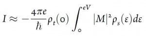
Furthermore, the matrix element |M|² is nearly energy-independent, and can be taken out of the integral to obtain:
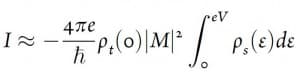
Assuming that the vacuum barrier between the tip and the sample is a simple square barrier, and applying WKB approximation, the matrix element |M|² can be written as:
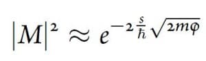
where m is the electron mass, s is the width of the vacuum barrier, and φ is the effective local barrier height, which represent some mixture of the tip and sample work functions. Using these, the final expression for the tunneling current that STM measures becomes:
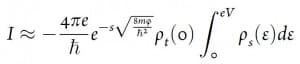
In summary, tunneling current measured by STM at bias V is proportional to the integral of the density of states of the sample from the Fermi level to eV.
Types of STM measurements
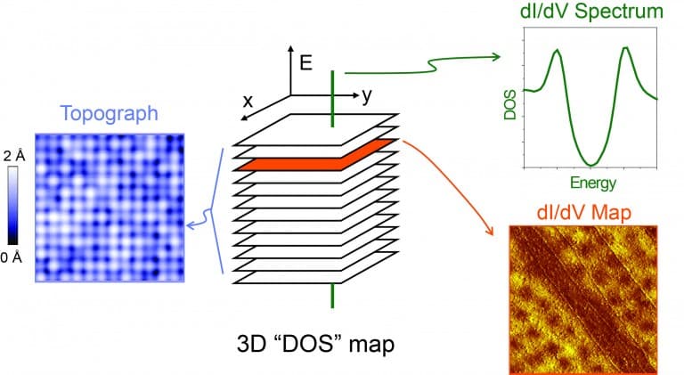
Figure 2. Schematic of 3-dimensional data sets obtained on a pixel grid (3D “DOS” maps) and main types of STM measurements.(i) Topograph is the most commonly acquired type of STM measurements, and allows us to visualize (to first approximation) the surface structure of the sample. It is acquired by rastering the tip across the sample at a fixed bias V, and adjusting the position of the tip in the z-direction to maintain the measured current at a fixed setpoint value.(ii) dI/dV spectrum is measured by positioning the tip in tunneling range (tunneling current non-zero) at any point on the sample, turning the feedback off, and measuring differential conductance dI/dV as a function of bias V. It is directly proportional to the density of states of the sample at energy e·V.(iii) dI/dV map allows us to visualize how differential conductance dI/dV vary spatially across the sample at a given energy (bias voltage V).
(1) Topograph
STM is most commonly used in the constant-current topographic mode. As the tip is rastered across the surface in the xy-plane at a fixed bias voltage V, the feedback loop adjusts the position of the tip in the z-direction to maintain the measured current at a fixed setpoint value. The z trajectory of the tip effectively maps the surface contour, thus producing the STM topograph (Figure 2).However, as seen in the previous section, tunneling current is dependent on tip sample separation as well as the integral of the density of states from Fermi level to eV. Therefore, for a sample with a homogenous DOS, this contour purely corresponds to the geometric surface corrugations. However, most materials exhibit a spatially heterogeneous DOS, which means that STM topographs of these compounds represent a combination of effects due to geometric corrugations and electronic density of states. An example of an STM topograph acquired on topological crystalline insulator SnTe (001) is shown in Figure 2.
(2) dI/dV spectrum
In addition to acquiring information about the surface geometry, STM can obtain electronic DOS at energies of up to several electron volts, both in occupied and unoccupied sample states. The measurement is done by turning off the feedback loop (which fixes the tip-sample distance s), sweeping the bias voltage V, and measuring the current response I(V). As tunneling current I is proportional to the integral of the density of states from Fermi level to eV, taking a numerical derivative yields DOS of the sample at a given energy eV:
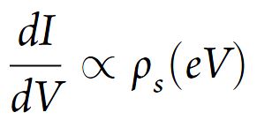
From a practical stand point, taking a numerical derivative of I vs. V$curve, to obtain the conductance dI/dV is extremely noisy. To circumvent this problem, dI/dV is usually measured using a lock-in amplifier technique, where a small bias voltage modulation dV (typically a few millivolts) is added to V, and the change in the tunneling current dI is measured to obtain dI/dV. An example of a typical dI/dV spectrum measured on the surface of a high-temperature superconductor Bi2Sr2CaCu2O8 is shown in Figure 2, and shows a gap in DOS.
(3) 3D “DOS” map and dI/dV map
dI/dV spectra can be obtained on a densely-spaced pixel grid, which results in a 3-dimensional data set often referred to as a “DOS map” (Figure 2). Extracting a single “slice” (dI/dV map) at any desired energy approximately reveals spatial distribution of the density of states. An example of a dI/dV map can be seen in Figure 2, and shows magnetic vortices in doped Fe-based high-temperature superconductor BaFe2As2.